Multiply and Accumulate Unit using Vedic Multiplier
| ✅ Paper Type: Free Essay | ✅ Subject: Engineering |
| ✅ Wordcount: 2324 words | ✅ Published: 31 Aug 2017 |
Design and Implementation of FPGA based 64 bit MA Cunitusing VEDIC Multiplier and Reversible Logic gates
ABSTRACT:
Now a days in VLSI technology size, power, and speed are the main constraints to design any circuits. In normal multipliers delay will be more and the number of computations also will be more. Because of that speed of the circuits designed with the normal multipliers will be low and it will consume more power.
This paper describes Multiply and Accumulate Unit using Vedic Multiplier and DKG reversible logic gates. The Vedic multiplier is designed by using Urdhava Triyagbhayam sutra and the adder design is done by using reversible logic to perform high speed operations. Reversible logic gates are also the essential constraint for the promising field of Quantum computing. The Urdhava Triyagbhayam multiplier is used for the multiplication function to reduce partial products in the multiplication process and to get high concert and less area .The reversible logic is used to get less power. The MAC is designed using Verilog code, simulation,synthesis is done in both RTL compiler using Xilinx and implemented on Spartan 3e FPGA Board.
KeyWords:MAC, Vedic multiplier, Reversible Gates
I. INTRODUCTION
Multiplication is the key in arithmetic operation and multiplier plays an important role in digital signal Processing. Unfortunately, the major source of power dissipation in digital signal processors is multipliers. In the past decade researchers developed multipliers with the help of CMOS logic which has all the disadvantages as discussed earlier. Therefore multipliers design for digital signal processing applications should be competent. So the proposed method is designed using pass logic principles, which shows improvements over CMOS designs. Pass logic principle based circuits are capable to accomplish superior performance in power, speed and area when implemented in VLSI[1]. Several case studies show that pass logic principle based design implements most functions with fewer transistors which reduces the overall capacitance than static CMOS; thus, resulting in low power and fast switching time. The Pass logic standard based design is a capable, due to its better performance in power consumption, area and speed.
thirty percent of the multiplier space is taken by the Booth encoder and selector logic [1-3]. So a improved design of Booth encoder and selector is essential. The main objective of this work is to design and implement new Booth encoders and selector logics which are hardware efficient and consequently power- aware.Various designs of these logic units are proposed in this work where the number of transistors needed are less when compared to previously designed units.The gate level implementations of these designs were tested for functionality using LoKon software gates (XNOR, XOR , NAND,NOR,AND,XOR-XNOR combination gate) and MUX used in these circuits were simulated and verified for functionality using TopSPICE. Due to the limitation in the numbers of transistor count in the TopSPICE, it was not capable to simulate the entire circuit in the transistor level. Further, these designs were used to build multiplier[2].
Multiplier is the need for higher word width for signal process applications. This design is scalable without any loss of merits. All the pass transistor circuits have been tested for fully restored voltage at the output[3]. Therefore, when these circuits are combined to form the whole multiplier voltage drop will not cause a problem.
II. LITERATURE REVIEW
Nareshnaik, SivaNagendra Reddy proposed “Design of Vedic Multiplier for Digital Signal Processing Applications”[1] .In this method design of adders is difficult and design may be complex and also its require more power.
Anitha, Sarath Kumar proposed “A 32 BIT MAC Unit Design Using Vedic Multiplier and Reversible Logic Gate” design.In this paper they designed for 32 bit Multiplier.But most of the multipliers used in Digital signal processing applications 64 bit multipliers.
So many researchers proposed many methods to design multipliers and adders.Among all the methods multiplier design with reversible logic gate design is the efficient method.In reversible gates also different reversible gate are available[4].Some researchers used Kogge stone Adders,some one used Toffiligates[5].DKG is the one of the gate used in the MAC design.This proposed method represents 64 bit MAC design using reversible logic gates.
III. PROPOSEDMETHOD
Multiply Accumulate (MAC) unit is designed by using Multipliers and adders both will be joined by an accumulate unit. The applications of MAC unit are Digital Signal Processors, microprocessors, and logic units and.MAC determines the speed and improves the performance of the entire system[6]. The proficient designs by MAC unit are Fast Fourier Transform(FFT/IFFT) ,Discrete Cosine Transform (DCT). Since, they are normally executed by inflexible application of multiplication and addition, the total system speed and performance depends on the speed of the addition and multiplication process speed in the system[7]. In most cases the delay in the architecture is due to the addition in parallel stages which we have to concentrate more to improve the speed. Finally we are going to compare our Vedic MAC unit with the Conventional MAC unit based on the parameters like Speed,area and power consumption[8].
A multiplying blockfunction can be conceded in threedifferent ways: conventional addition, partial product addition (PPA) and finally partial product Generation (PPG). The two bud vase materials that must be considered are raising the speed of MAC which is accumulator block partial and product reduction[9]. The 64 bit MAC design which will make use of Vedic multiplier and reversible logic gate can be accomplished in two stages. Firstly, multiplier stage, where a usual multiplier is replaced by Vedic multiplier using UrdhavaTriyagbhayam sutra from Vedic Mathematics.Multiplication is the primary operation of MAC unit. Speed, area, Power dissipation, consumptionand latency are the major concerns in the multiplier stage. So, to evade them, we will go for fast multipliers in different applications of DSP, networking, etc. There are mostly two major criterions that can possibly improve speed of the MAC units are sinking the partial products and because of that accumulator yoke is getting decreased. To perform the multiplication of N*N it requires approximately 2N-1 cross products of different widths and (log2N + 1) partial products. The partial products are obtained from Urdhava sutra is by Criss Cross Method. The maximum number of bits in partial products will lead to Critical path. The second part of MAC is Reversible logic gate. Loss of every bit of information in the computations that are not reversible is kT*log2 joules of heat energy are generated, where k is Boltzmann’s constant and T the absolute temperature at which computation is performed.
IV. DESIGN OF MAC ARCHITECTURE
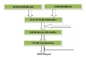 Fig 1: MAC Architecture
The design of MAC architecture consists of 3 sub designs.
- Design of 64 X 64 bit Vedic Multiplier.
- Design of 128 bit DKG adder
- Design of Accumulator which integrates both multiplier and adder stages.
Vedic Multiplier
Vedic Mathematics is part of four Vedas (books of wisdom). It is part of Sthapatya- Veda (book on civil engineering and architecture), which is an upa- veda (supplement) of Atharva Veda.
Vedic Mathematics existed in ancient India and was revived by a popular mathematician, Sri Bharati Krishna Tirthaji. He divided Vedic mathematics into sixteen formulae(sutras). These formulae deal with Algebra, Analytical Geometry, Algebra, Trigonometry, Geometry etc. The ease in the Vedic mathematics sutras covers way for its application in several prominent domains of engineering like Signal Processing, VLSI and Control Engineering .
1) (Anurupye) Shunyamanyat
2) ChalanaKalanabyham
3) EkadhikinaPurvena
4) EkanyunenaPurvena
5) Gunakasamuchyah
6) Gunitasamuchyah
7) NikhilamNavatashcaramamDashatah
8) ParaavartyaYojayet
9) Puranapuranabyham
10) Sankalana- vyavakalanabhyam
11) ShesanyankenaCharamena
12) ShunyamSaamyasamuccaye
13) Sopaantyadvayamantyam
14) Urdhva-tiryakbhyam
15) Vyashtisamanstih
16) Yaavadunam
Vedic Maths can be divided into sixteen different sutras to perform mathematical operations. Among these surtras the Urdhwa Tiryakbhyam Sutra is one of the most highly preferred algorithms for performing multiplication[11-14]. The algorithm is competent enough to be employed for the multiplication of integers as well as binary numbers. The term “UrdhwaTiryakbhyam” originated from 2
Sanskrit words Urdhwa and Tiryakbhyam which mean “vertically” and “crosswise” respectively.The mainadvantage of utilizing this algorithm in comparison with the existing multiplication techniques, is the fact that it utilizes only logical “AND” operations, half adders and full adders to complete the multiplication operation. Also, the partial products required for multiplication are generated in parallel and apriority to the actual addition thus saving a lot of processing time[15-17].
UrdhwaTiryakbhyam Algorithm
Let us consider two eight bit numbers X(7:0) and Y(7:0) , where 7 signify Most Significant Bit and 0 represent Least Significant Bit. P0 to P15 signify each bit of the final computed product. It can be seen from equation (1) to (15), that P0 to P15 are calculated by adding partial products, which are calculated previously using the logical AND operation.
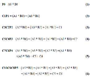 The individual bits obtained from equations (1) to equation (15), in turn when concatenated produce the final product of multiplication which is represented in equation (16).The carry bits generated during the computation of the individual bits of the final product are represented from C(1) to C(30). The carry bits generated in (14) and (15) are ignored since they are redundant.
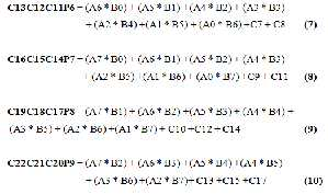
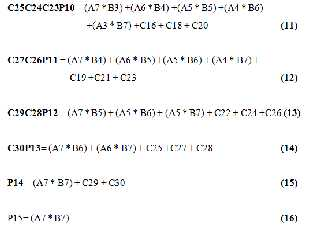
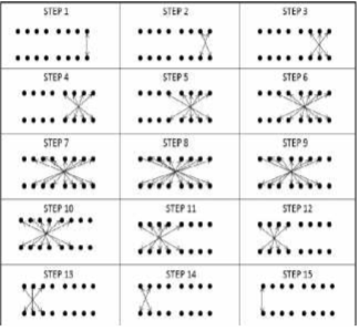 Fig 2 : Pictorial Illustration of UrdhwaTiryakbhyam
Sutra
Graphically exemplifies the step by step procedure of multiplying two eight bit numbers using the Urdhwa Tiryakbyam Vedic Multiplication Sutra[20]. The black circles specify the bits of the multiplier and multiplicand, and the two-way arrows specify the bits to be multiplied in order to arrive at the
individual bits of the final product. The hardware architecture of the 8×8 Urdhwa multiplier has been designed and shown in Fig 2.
ï‚· Lowest quantum cost
DKG Gate
A 4 X 4 reversible DKG gate that preserve
work singly as a reversible full adder and parallel adder is shown in below fig 5. If input A is zero, the DKG gate performed Full adder operation, and if input A is 1 then reversible logic gate performed Full subtractor operation. It has been confirmed that a reversible full- adder circuit requires at least two or three garbage outputs to make the distinctive[10][19].
output combinations
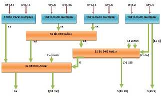 Fig 3: 32 Ã-32 Vedic multiplier using 16 Ã- 16 Vedic multiplier
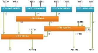 Fig 4: 64Ã- 64 Vedic multiplier using 32x32Vedic multiplier
V. DESIGN OF ADDERUSING
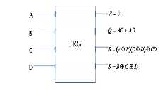 Fig. 5a DKG gate
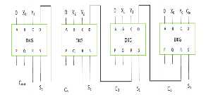 Fig. 5b Parallel adder using DKG gate
AccumulatorStage:
Accumulator has an significant role in the DSP
applications in different ranges. The register designed
REVERSIBLE LOGICDKGGATE
in the accumulator is used
to add the multiplied
Reversible logic is a distinct method diverse from other logic). Loss of information is not probable
numbers. Multiplier, adder and an accumulator are
forming the vital establishment for the MAC unit. The conventional MAC unit has a multiplic and and here. In this logic, the numbers of outputs are identical multiplier to do the basic multiplication and some to the number of inputs.
General consideration for reversible logicgate
parallel adders to add the partial products generated in the previous step. To get the final multiplication output A Boolean function is reversible if and only if we add the partial product to these results. Vedic all the values in the input set can be mapped with a single value in the output position. Landauer and Multiplier has put forward to intensify the action of the MAC Unit.
Bennet both demonstrated that conventional irreversible circuits will the usage of construct us to
VI. RESULTS AND DISCUSSION
power dissipation a circuit consisting of only reversible gates does not dissipate power. The following points necessity be reserved in mind to realize an optimized circuit:
ï‚· Loops are not authorized
ï‚· Minimum delay
ï‚· Zero energy dissipation
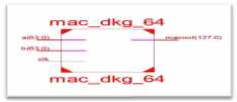 Fig 6: RTL Schematic of MAC Unit
ï‚· Fan-out is not authorized
The modified 64 bit multiplier using Vedic
ï‚· Garbage outputs must be small multiplier and DKG adder is fast and design of MAC done using Xilinx.
The above fig 7shows comparison between Verilog code using Xilinx. The below fig 6 shows the
 RTL Schematic of the proposed design.
Logic Utilization
70000
No.of Slice FlipFlops
60000
No.of 4 input LUTs
50000
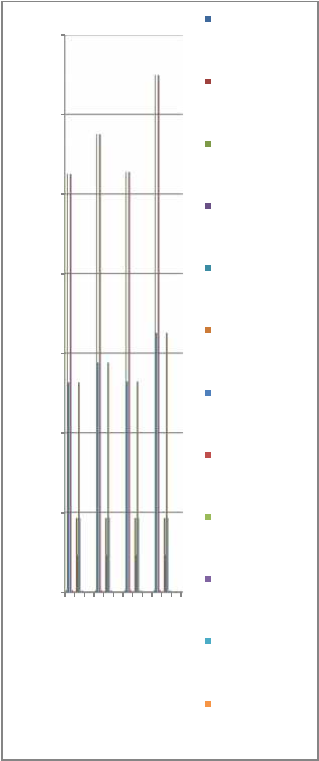
MAC design unit using different Adders. The number of LUTs and utilization of logic blocks in MAC design using CSA, RCA, KSA will be greater than DKG and speed is also more in MAC design using DKG. But it will take more area.
Compare to array multipliers, baugh wooley multipliers and booths multipliers Vedic multipliers requires less area and performs operations at high speed.
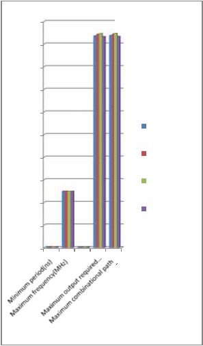
The below fig 8 shows the statistics results of
MAC design Vedic Multiplier with different adders. In which DKG Adders has moderate delay. But it consumes very less power and it can be designed in small area.
40000
Number of occupied
Slices
Number of Slices containing only related logic
1000
900
800
30000
20000
10000
Number of Slices containing unrelated logic
Total Number of 4 input LUTs
Number used as logic
Number used as Shift
Registers
700
600
500
400
 300
300
200
100
MAC Design using RCA
MAC Design using CSA
MAC Design using KSA
MAC Design using DKG
0
Number of nonded
0 IOBs
Number of
BUFGMUXs

 Average Fanout of non-Clock Nets
Fig7: Synthesis report of 64-bit MAC using Vedic Multiplier using RCA,DKG and KSA Reversible logic gates
Fig8: Delay Analysis report of 64-bit MAC using Vedic Multiplier using RCA,DKG and KSA Reversible logic gates
in table 2. By Combining the Vedic and reversible logic will direct to new and competent attainments in developing various fields of digital signal processing Applications.
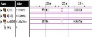 Fig 9: Simulation result of Adder
The above fig 9 shows that simulation result of DKG adder. It is a 32 bit adder. In this design we used two 64 bit adders. This adder has two inputs a and b
,two outputs sum and carry. For adder a =19997091 and b= 0001fffdapplied.Which results sum is
0199b708e and carry is 0.
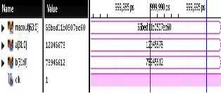
Fig 10: Vedic Multiplier result of 64 bit MAC unit
The above fig 10 shows the simulation result of 64 bit MAC design unit. For this design we applied two inputs. In which values are a=12345678 and b=78945612 and it will give result of
55bed11b057ec60.
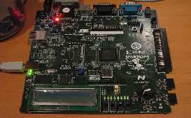
Fig 11: Vedic Multiplier result of 64 bit MAC unit on
FPGA
CONCLUSION AND FUTURE SCOPE
The results of this proposed 64 bit Urdhava
Triyagbhayam Vedic multiplier with DKG adder are quite good. Design of MAC unit structure and its performance has been scrutinize for all the blocks. Therefore, the 64-bit Urdhava Triyagbhayam sutra Multiplier and reversible logic is the best in all aspects like speed power product ,delay, area and complication
as compared to all other architectures which are shown
Cite This Work
To export a reference to this article please select a referencing stye below:
Related Services
View all


DMCA / Removal Request
If you are the original writer of this essay and no longer wish to have your work published on UKEssays.com then please click the following link to email our support team:
Request essay removal